NFV and SDN: What’s the Difference?

NFV and SDN: What’s the Difference?

NFV Network Functions Virtualization Overture Networks

Software-defined networking (SDN) and network function virtualization (NFV) are hot topics. They are clearly related, but how exactly are they similar? How are they different? How do they complement each other? Are you new to SDN or NFV? Check out SDNCentral’s SDN and NFV Essentials to learn the basics.

SDN – Born on the Campus, Matured in the Data Center

SDN got its start on campus networks. As researchers were experimenting with new protocols they were frustrated the need to change the software in the network devices each time they wanted to try a new approach. They came up with the idea of making the behavior of the network devices programmable, and allowing them to be controlled by a central element. This lead to a formalization of the principle elements that define SDN today:

  • Separation of control and forwarding functions
  • Centralization of control
  • Ability to program the behavior of the network using well-defined interfaces

The next area of success for SDN was in cloud data centers. As the size and scope of these data centers expanded it became clear that a better way was needed to connect and control the explosion of virtual machines. The principles of SDN soon showed promise in improving how data centers could be controlled.

Interested in learning more about network functions virtualization and software-defined networking? Be sure to check out our pages on NFV for Dummies SeriesNFV MANO, ETSI ISG NFVOPNFV, and Virtual Network Functions.

OpenFlow – Driving Towards Standards

So, where does OpenFlow come into the picture? As SDN started to gain more prominence it became clear that standardization was needed. The Open Networking Forum (ONF) [1] was organized for the purpose of formalizing one approach for controllers talking to network elements, and that approach is OpenFlow. OpenFlow defines both a model for how traffic is organized into flows, and how those flows can be controlled as needed. This was a big step forward in realizing the benefits of SDN. [Editor’s Note (11/6/14): In addition to ONF, the OpenDaylight Project also aims to advance open standards and SDN adoption. Announced in April 2013 by the Linux Foundation, the OpenDaylight Project’s goal is to offer a functional SDN platform that gives users directly deployed SDN without the need for other components. In addition to this, contributors and vendors can deliver add-ons and other pieces that will offer more value to OpenDaylight.]

NFV – Created by Service Providers

Whereas SDN was created by researchers and data center architects, NFV was created by a consortium of service providers. [Editor’s Note (11/6/14): Service providers attempted to speed up deployment of new network services in order to advance their revenue and growth plans, and they found that hardware-based appliances limited their ability to achieve these goals. They looked to standard IT virtualization technologies and found NFV helped accelerate service innovation and provisioning. With this, several providers banded together and created the European Telecommunications Standards Institute (ETSI). The creation of ETSI resulted in the foundation of NFV’s basic requirements and architecture.] The original NFV white paper [2] describes the problems that they are facing, along with their proposed solution:

Network Operators’ networks are populated with a large and increasing variety of proprietary hardware appliances. To launch a new network service often requires yet another variety and finding the space and power to accommodate these boxes is becoming increasingly difficult; compounded by the increasing costs of energy, capital investment challenges and the rarity of skills necessary to design, integrate and operate increasingly complex hardware-based appliances. Moreover, hardware-based appliances rapidly reach end of life, requiring much of the procure-design-integrate-deploy cycle to be repeated with little or no revenue benefit.

Network Functions Virtualisation aims to address these problems by leveraging standard IT virtualisation technology to consolidate many network equipment types onto industry standard high volume servers, switches and storage, which could be located in Datacentres, Network Nodes and in the end user premises. We believe Network Functions Virtualisation is applicable to any data plane packet processing and control plane function in fixed and mobile network infrastructures.

[Editor’s Note (11/6/14): ETSI continues to address NFV innovation. In September 2014, the Linux Foundation announced another open source reference platform — the Open Platform for NFV Project (OPNFV). OPNFV will work closely with ETSI and others to press for consistent implementation of open standards.]

SDN versus NFV

Now, let’s turn to the relationship between you SDN and NFV. The original NFV white paper [2] gives an overview of the relationship between SDN and NFV:

As shown in Figure 1, Network Functions Virtualization is highly complementary to Software Defined Networking (SDN), but not dependent on it (or vice-versa). Network Functions Virtualization can be implemented without a SDN being required, although the two concepts and solutions can be combined and potentially greater value accrued.

Network Functions Virtualisation Relationship with SDN

Figure 1. Network Functions Virtualisation Relationship with SDN

Network Functions Virtualisation goals can be achieved using non-SDN mechanisms, relying on the techniques currently in use in many datacentres. But approaches relying on the separation of the control and data forwarding planes as proposed by SDN can enhance performance, simplify compatibility with existing deployments, and facilitate operation and maintenance procedures. Network Functions Virtualization is able to support SDN by providing the infrastructure upon which the SDN software can be run. Furthermore, Network Functions Virtualization aligns closely with the SDN objectives to use commodity servers and switches.

SDN and NFV – Working Together?

Let’s look at an example of how SDN and NFV could work together. First, Figure 2 shows how a managed router service is implemented today, using a router at the customer site.

Managed Router Service Today

Figure 2: Managed Router Service Today

NFV would be applied to this situation by virtualizing the router function, as shown in Figure 3. All that is left at the customer site is a Network Interface Device (NID) for providing a point of demarcation as well as for measuring performance.

Managed Router Service Using NFV

Figure 3: Managed Router Service Using NFV

Finally, SDN is introduced to separate the control and data, as shown in Figure 4. Now, the data packets are forwarded by an optimized data plane, while the routing (control plane) function is running in a virtual machine running in a rack mount server.

Managed Router Service Using NFV and SDN

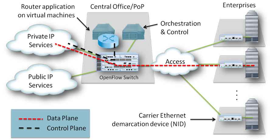
Figure 4: Managed Router Service Using NFV and SDN

The combination of SDN and NFV shown in Figure 4 provides an optimum solution:

  • An expensive and dedicated appliance is replaced by generic hardware and advanced software.
  • The software control plane is moved from an expensive location (in dedicated platform) to an optimized location (server in a data center or POP).
  • The control of the data plane has been abstracted and standardized, allowing for network and application evolution without the need for upgrades of network devices.

Summary

The table below provides a brief comparison of some of the key points:

Category

SDN

NFV

Reason for Being Separation of control and data, centralization of control and programmability of network Relocation of network functions from dedicated appliances to generic servers
Target Location Campus, data center / cloud Service provider network
Target Devices Commodity servers and switches Commodity servers and switches
Initial Applications Cloud orchestration and networking Routers, firewalls, gateways, CDN, WAN accelerators, SLA assurance
New Protocols OpenFlow None yet
Formalization Open Networking Forum (ONF) ETSI NFV Working Group

Source: NFV and SDN: What’s the Difference?

NFV and SDN: What’s the Difference? was last modified: July 13th, 2017 by Jovan Stosic

The Gypsy Baron

The Gypsy Baron (German: Der Zigeunerbaron) is an operetta in three acts by Johann Strauss II which premiered at the Theater an der Wien on 24 October 1885. Its libretto was by the author Ignaz Schnitzer (de) and in turn was based on Sáffi by Mór Jókai. During the composer’s lifetime, the operetta enjoyed great success, second only to the popularity of Die Fledermaus. The scoring and the nature of Strauss’s music have also led many music critics to consider this work a comic opera or a lyric opera.

Its genesis was rather swift and smooth, as Strauss was no stranger to the Hungarian influences apparent in the music score. Many of his earlier works also bore many similar themes, such as the polka Éljen a Magyar! (“Long live the Hungarians!”), Op. 332. Originally, Strauss and Schnitzer intended the operetta as an opera but further revisions were made and the idea of a comic opera was conceived.

Strauss’s work on the operetta was interrupted in autumn 1883 due to nicotine poisoning and fainting fits and he was to recuperate in Franzensbad. Strauss work on the act 3 of the work was also interrupted when his third wife, Adele Strauss, was taken ill and the couple left for Ostend. Not until autumn 1885 was the work finally completed, with Schnitzer making various revisions of the libretto to suit Strauss’s style of composing which were not present in the latter’s previous stage works.

Source: The Gypsy Baron – Wikipedia

The Gypsy Baron was last modified: September 25th, 2017 by Jovan Stosic

antenna – What will it take to build a DIY 2km (city conditions) RF transmitter (433Mhz)? – Electrical Engineering Stack Exchange

Source: antenna – What will it take to build a DIY 2km (city conditions) RF transmitter (433Mhz)? – Electrical Engineering Stack Exchange

antenna – What will it take to build a DIY 2km (city conditions) RF transmitter (433Mhz)? – Electrical Engineering Stack Exchange was last modified: July 13th, 2017 by Jovan Stosic

Question #124157 : Questions : Inkscape

I imported a drawing in white text on black background. I want black text on white background.
Help?

1 – Draw a BLACK rectangle the same size as the imported drawing.

2 – move the rectangle drawn so it covers your imported drawing, then press Page Down to Make sure the imported drawing IS      the layer on top

3 – Select your imported drawing then hold shift key down and select the black rectangle you drew.

4 – From the top menu select Object->Mask->Set You will have all your white text now in black on a white back ground.

Source: Question #124157 : Questions : Inkscape

Question #124157 : Questions : Inkscape was last modified: July 13th, 2017 by Jovan Stosic

Electronics Forum -> Fr-2 Vs Fr-4 Pcb Material

I’m going to purchase some Kinsten presensitised PCBs for making my own PCBs (UV photoresist method), and they come in two varieties; normal fibreglass (FR-4), and another material called ‘paper phenolic’ (FR-2).
I’ve never used FR-2 for PCB designs before, but looking on Wikipedia’s page for it, it states that FR-2 is a bit less mechanically robust:

Source: Electronics Forum -> Fr-2 Vs Fr-4 Pcb Material

Electronics Forum -> Fr-2 Vs Fr-4 Pcb Material was last modified: July 13th, 2017 by Jovan Stosic

Best Practice: HCl + H2O2 PCB etching (Hydrogen peroxide & hydrochloric acid) – Page 1

Safety

VERY WELL VENTILATED environment!! I did it on my balcony. Do not do this in closed space. Chlorine gas is very nasty and partial pressure of Chlorine is SURPRISINGLY high! 24 % HCl fumes is on the brink of nasty. DO take this seriously. If you don’t care about your lungs, eyes and other exposed body parts: consider all metal fixtures and equipment around you. It WILL corrode from the fumes. And very quickly.
USE YOUR SAFETY GLASSES!
USE GLOVES!! Both are really cheap.
Start with small patches of copper.
MARK the containers. ALL of them. With permanent markers. So that you cannot oversee it. Even if only water is in them. Especially since you are (I am) doing that at home – your noodles might taste funny when you accidentally use that food container again….
DO NOT do it in your kitchen, near food, your son’s / daughter’s bedroom and so on. Best in a workshop or outside. Not your dinner table, not your couch. Chemistry can be bad sometimes.
READ the damn Materials Safety Datasheets (MSDS). Print them out, read them 10 times. Try and remember what it says. It is important. Really is. I mean… REALLY. And read them every time you start doing your thing. Especially when you do something new.

MSDS
HCl:
http://www.sciencelab.com/msds.php?msdsId=9924285

H2O2:
http://www.sciencelab.com/msds.php?msdsId=9924301

Acetone:
http://www.sciencelab.com/msds.php?msdsId=9927062

CuCk2:
http://www.ch.ntu.edu.tw/~genchem99/msds/exp22/CuCl2.pdf

H2O
Just to be safe: Don’t try and drink the deionized water. You might die of hyposalinity if you drink enough of it  :)

The chemistry
(please, correct if I am wrong – I did not have the time to look everything up right today):

H2O2 (aq)+ 2 HCL (aq) + Cu -> 2 H2O + Cu2+(aq) + 2 Cl (aq)

While the H2O2 serves as oxidant, I guess.
As far as I remember, Cu is almost inert to low(er) HCl-concentrations (<30 %).
So I’ll be bold and guess that H2O2 could work as a pure initiator (ergo, really small amounts may suffice?).

Materials
See attached picture for some of the materials I used.

1x 10 L PP container with screw cap
1x PP funnel
2x PP beakers, 20 ml, with 2 ml markings
2x PP 0.5 L food containers
1x Polymer tweezers (I used steel, but it’ll dessolve 🙂 )
1x safety goggles (DO use these! Cheap to buy, very valuable when you want to scratch your itchy eye….)
1x big box of cheap disposable vinyl gloves (Nitrile are more versatile. Vinyl will dissolve in Acetone, but are good for Oxidizing agents like HCl. Since I don’t mind the acetone, I chose vinyl. Also I like the feel better. Don’t buy Latex. They rip and puncture easily, plus they are expensive)
1x 7.8 M HCl (^= 24 %)
1x 8.8 M H2O2 (^=40 %)
1x pack of NaOH (I just used baking soda)
1x Acetone
1x Distilled / deionized water (really, tap water is just fine. But I am a sucker for best practice)
1x roll of packing tape (I just used it to mask one side of the dual sided copper clad board)
1x tin shears (for your copper clad boards)
1x steel wool
Xx permanent markers (Just for the try-out)
Xx strips of your copper clad board, FR4 (don’t start with an entire board right away. I tried a strip first to get a feeling)
Xx Paper wipes

Steps

cut small strips of copper clad PCB board with large tin shears.
abrasively cleaned surface with steel wool
thoroughly cleaned with acetone and paper wipes
made markings with permanent markers: different widths / areas, geometric forms and layer thicknesses
masked / covered areas (backside) of PCB strip that were not to be etched
Added cold tap water into 1st PP container

added into 2nd PP container as follows:

1st try:

  • Room temperature (~20 °C)
  • HCl, 24 %, 10 ml
  • H2O2, 40 % ~2ml

2nd try:

  • Room temperature (~20 °C)
  • deionized water, 15 ml
  • HCl, 7.8 M 24 %, 10 ml
  • H2O2, 8.8 M 40 % ~2ml

Added cold tap water into 1st PP food container
Added following chemicals into 2nd PP food container

After each try, I neutralized the solution with NaOH (baking soda in that case) and diluted it a little with some tap water and put it into a small PET bottle. I marked the bottle with a label and will get rid of it at a local chemical waste disposal service some time soon.

Results

1st try
Some 3 second etching.
Very fast. Very reactive.
Some over-etching apparent.
transparent green solution remains

2nd try:
Maybe 10 – 15 seconds of etching. But not as exothermic as the first try.
Reaction easier to control.
transparent green solution remains
over etching not apparent (at least from what I can tell… )
One “layer” of permanent marker seemed to be enough if no blank spots were left.
Thin lines were apparently not over-etched

TODO

1: reaction control
Control reaction speed. I will try:

  • controlling H2O2 addition
  • diluting (although I guess controlling reduction agent may be better – HCl is slow with Cu anyway)
  • pure water and control reactants (dripping in oxidant and reduction agent equally)

2.: Waste management
Find a way to easily neutralize the solution so that I can just safely pour it down the drain.
I’ll check on that. If anyone is interested, let me know

3.: Alternatives
I really do not want to bother with FeCl. It’s a mess.

I had in mind to try and do it galvanically. BUT: What do I do when a part of the board is “etched” away and there is a gap between two parts? I still need a physical, conducting connection between parts that are to be removed. Maybe there is some solution to this out there. Cannot think of anything, though. probably stupid idea. But I like the idea of an electro-chemical approach to the problem – no nasty chemicals, quick, controllable, broad error margin, safe, clean, etc….

I don’t have the space for milling. So not an option. Also high CAPEX and inefficient (not that I’ll be producing 10’000 boards a day. Probably I’ll make 10 my entire life 🙂

4.: learn to actually design a PCB  :-DD
Never did it. Let’s see what I do first. I ordered a LOT of SMD-stuff from China. So far I only played with through-hole and DIP on prototyping boards & breadboards.
My first project is an Atmega238 fast auto-ranging and not all too precise ohmmeter (I called the project SpeedyOHMalez here in the forum, hehe) for sorting resistors.

5.: Solder mask & silk screening
I ordered UV paint for the solder mask (nice red). I’ve read a little. I am curious to see how I manage to coat the board evenly.
Need a UV light (anyone in Switzerland has an unused one lying around?) and to study curing time, temperature resistance, etc.

Also I want to find out the best way to apply the “silk screen” on top of the solder mask. I saw a lot of actual silk screening.
Since I’ll only make one-offs for starters, I really don’t want to make an actual silk screen just for one design. I was thinking: Same process as the solder mask, just inverted, no? so: covering the entire board in (in this case white) UV curing paint, put laser printed mask over it (inverted) and wash the other stuff off. Not very material efficient… but it should work, no?

postscriptum:
I will try and make a complete tutorial out of this as I progress (and when I find the time). I want it to be a little more than the usual “pour this into this” you can find everywhere. Any help, comment, addition, constructive criticism ….. etc…. is much appreciated. Especially if I got things wrong. I’d generally like to stick to HCl as oxidizing agent. It is readily available and cheap.
There are safety issues with this, sure. But I think ignorance is a great tragedy and people should be educated – that should also involve properly handling hazardous chemicals.


Source: https://www.eevblog.com/forum/projects/best-practice-hcl-h2o2-pcb-etching-(hyrogen-peroxide-hydrochloric-acid)/

Best Practice: HCl + H2O2 PCB etching (Hydrogen peroxide & hydrochloric acid) – Page 1 was last modified: September 9th, 2017 by Jovan Stosic